- 您现在的位置:买卖IC网 > Sheet目录1252 > V2DIP1-64 (FTDI, Future Technology Devices International Ltd)MOD VINCULUM-II DEV 1 PORT 64DIP
�� �
�
�Document� Reference� No.:� FT_000165�
�V2DIP1-64� VNCL2-64Q� Development� Module� Datasheet� Version� 1.01�
�Clearance� No.:� FTDI#� 154�
�3.8� Debugger� Interface�
�The� purpose� of� the� debugger� interface� is� to� provide� access� to� the� VNC2� silicon/firmware� debugger.� The�
�debug� interface� can� be� accessed� via� the� appropriate� pin� on� the� DIL� connector� or� more� easily,� it� can� be�
�accessed� by� connecting� a� debug� module� to� the� J3� connector.� This� debug� module� will� give� access� to� the�
�debugger� through� a� USB� connection� to� a� PC� via� the� Integrated� Development� Environment� (IDE).� The� IDE�
�is� a� graphical� interface� to� the� VNC2� software� development� tool-chain� and� gives� the� following� debug�
�capabilities� through� the� debugger� interface:�
�Flash� Erase,� Write� and� Program.�
�Application� debug� -� application� code� can� have� breakpoints,� be� single� stepped� and� can� be� halted.�
�Detailed� internal� debug� -� memory� and� register� read/write� access.�
�The� Debugger� Interface,� and� how� to� use� it,� is� further� described� in� the� following� applications� Note�
��3.8.1� ignal� Description� -� Debugger� Interface�
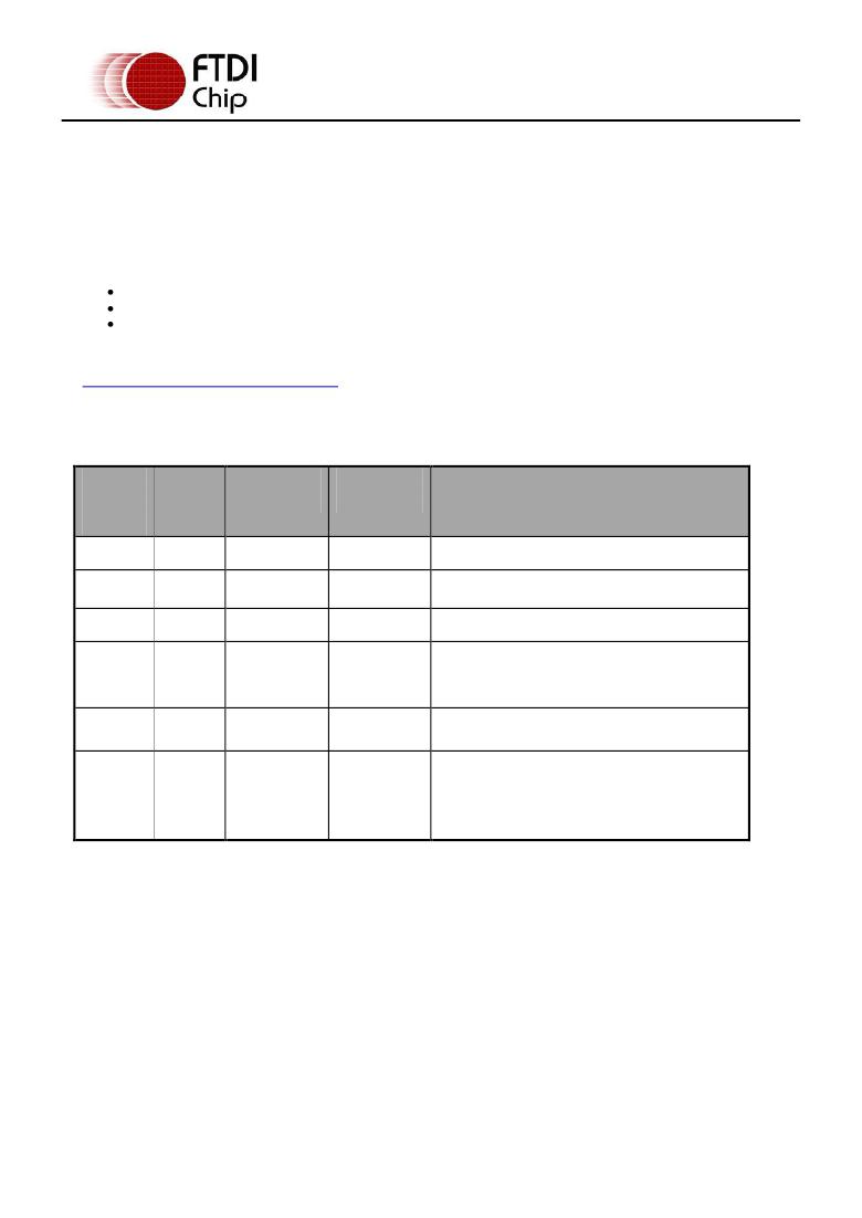
�Table� 3.10� shows� the� signals� and� pins� description� for� the� Debugger� Interface� pin� header� J3�
�Name�
�Pin� No.�
�J3-1�
�J3-2�
�J3-3�
�J3-4�
�J3-5�
�J3-6�
�Name�
�IO0�
�-�
�GND�
�RESET#�
�PROG#�
�5V0�
�On� PCB�
�DBG�
�[Key]�
�GND�
�RST#�
�PRG#�
�VCC�
�Type�
�I/O�
�-�
�PWR�
�Input�
�Input�
�PWR� Input�
�Description�
�Debugger� Interface�
�Not� connected.� Used� to� make� sure� that� the� debug�
�module� is� connected� correctly.�
�Module� ground� supply� pin�
�Can� be� used� by� an� external� device� to� reset� the�
�VNCL2.� This� pin� is� also� used� in� combination� with�
�PROG#� and� the� UART� interface� to� program�
�firmware� into� the� VNC2.�
�This� pin� is� used� in� combination� with� the� RESET#�
�pin� and� the� UART� interface� to� program� firmware�
�into� the� VNC2.�
�5.0V� module� supply� pin.� This� pin� can� be� used� to�
�provide� the� 5.0V� input� to� the� V2DIP1-64� from� the�
�debugger� interface� when� the� V2DIP1-64� is� not�
�powered� from� the� USB� connector� (VBUs)� or� the�
�DIL� connector� pins� J1-12,� J1-13� and� J1-19� and�
�J3-6.�
�Table� 3.10� -� Signal� Name� and� Description� –� Debugger� Interface�
�Copyright� ?� 2010� Future� Technology� Devices� International� Limited�
�17�
�发布紧急采购,3分钟左右您将得到回复。
相关PDF资料
V2DIP2-32
MOD VINCULUM-II DEV 2 PORT 32DIP
V2DIP2-48
MOD VINCULUM-II DEV 2 PORT 48DIP
V2DIP2-64
MOD VINCULUM-II DEV 2 PORT 64DIP
V2F118X500Y3DDP
VARISTOR CAP FEEDTHRU 50V 0805
V5.5MLA020164NR
VARISTOR ESD 5.5V 64PF SMD 0201
V751NA34
VARISTR IND SQ DISC 750V 34MM NA
VA200060K121DL
VARISTOR TVS 60VDC 300A AXIAL
VAR-18120550M5P-XK
VARISTOR RING 55V 12MM 5-TERM
相关代理商/技术参数
V2DIP2-32
功能描述:界面开发工具 USB Vinculum-II 32 Pin Mod 2 USB Ports
RoHS:否 制造商:Bourns 产品:Evaluation Boards 类型:RS-485 工具用于评估:ADM3485E 接口类型:RS-485 工作电源电压:3.3 V
V2DIP2-48
功能描述:界面开发工具 USB Vinculum-II 48 Pin Mod 2 USB Ports
RoHS:否 制造商:Bourns 产品:Evaluation Boards 类型:RS-485 工具用于评估:ADM3485E 接口类型:RS-485 工作电源电压:3.3 V
V2DIP2-64
功能描述:界面开发工具 USB Vinculum-II 64 Pin Mod 2 USB Ports
RoHS:否 制造商:Bourns 产品:Evaluation Boards 类型:RS-485 工具用于评估:ADM3485E 接口类型:RS-485 工作电源电压:3.3 V
V2E4-TA02
功能描述:电源管理IC开发工具 Random Vibe Module
RoHS:否 制造商:Maxim Integrated 产品:Evaluation Kits 类型:Battery Management 工具用于评估:MAX17710GB 输入电压: 输出电压:1.8 V
V2-EVAL
功能描述:MOD VINCULUM-II EVAL KIT RoHS:是 类别:编程器,开发系统 >> 评估演示板和套件 系列:Vinculum-II 标准包装:1 系列:- 主要目的:数字电位器 嵌入式:- 已用 IC / 零件:AD5258 主要属性:- 次要属性:- 已供物品:板 相关产品:AD5258BRMZ1-ND - IC POT DGTL I2C1K 64P 10MSOPAD5258BRMZ10-ND - IC POT DGTL I2C 10K 64P 10MSOPAD5258BRMZ100-ND - IC POT DGTL I2C 100K 64P 10MSOPAD5258BRMZ50-ND - IC POT DGTL I2C 50K 64P 10MSOPAD5258BRMZ1-R7-ND - IC POT DGTL I2C 1K 64P 10MSOPAD5258BRMZ10-R7-ND - IC POT DGTL I2C 10K 64P 10MSOPAD5258BRMZ50-R7-ND - IC POT DGTL I2C 50K 64P 10MSOPAD5258BRMZ100-R7-ND - IC POT DGTL I2C 100K 64P 10MSOP
V2-EVAL (EU)
功能描述:界面开发工具 USB Vinculum-II Eval Kit EU Power Supply RoHS:否 制造商:Bourns 产品:Evaluation Boards 类型:RS-485 工具用于评估:ADM3485E 接口类型:RS-485 工作电源电压:3.3 V
V2-EVAL (JP)
制造商:Future Technology Devices International (FTDI Chip) 功能描述:VINCULUM II EVALUATION BOARD
V2-EVAL (JPN)
功能描述:界面开发工具 USB Vinculum-II Eval Kit JP Power Supply RoHS:否 制造商:Bourns 产品:Evaluation Boards 类型:RS-485 工具用于评估:ADM3485E 接口类型:RS-485 工作电源电压:3.3 V